Specifications and Results
Specifications Overview
For the Micro P’s Project, the specifications are as follows:
- Audibly implements the intended effect.
- Physical switch can toggle the audio effect applied to the input.
- I2S is used to communicate between the MCU and FPGA.
- The MCU collects samples from the guitar.
- FPGA incorporates the DSP block to implement the intended effect on sampled audio.
- DAC outputs signal compatible with a guitar amplifier.
Technical Requirements Checklist:
- Smooth
- Proper amplitude
- AC-coupled
- Proper analog input protection and filtering
- 3.3V voltage clamping
- Bypass capacitance
- Unity gain buffer
- Anti-aliasing filter
- Gain
Results:
Audibly Implements the Intended Effect
- Status: The system audibly implements the intended effect.
- Effect details: The project implements a chorus effect. This works by duplicating a sample into a “wet” and “dry” sample and mixing them. The wet sample is stored in memory and delayed by a varying amount determined by a low-frequency oscillator (LFO).
- Implementation: The chorus was implemented on the FPGA using a circular delay buffer module and an LFO module to generate the wet sample, followed by a simple 50% mix of both wet and dry signals.
Physical Switch Toggles Audio Effect
- Goal: To toggle between the desired effect and a normal output. This allows listeners to audibly distinguish between the implemented effect and the regular guitar output.
- Implementation: A button serves as a system bypass.
- Mechanism: Instead of routing the analog guitar wave through the MCU and FPGA, the system bypasses it directly to the amp. This allows for distinguishing between the two signals.
I2S Communication
- Usage: I2S is used for communication between the MCU and FPGA.
- Function: The MCU sends sampled waves (converted from analog guitar input) to the FPGA to handle the chorus effect.
- Protocol: Communication is established via the SAI module using I2S. This allows for two-channel digital audio transmission as Pulse Code Modulation (PCM), which is essential for high-quality audio.
- Signals: The protocol uses Serial Clock (SCK), Word Select (WS), and Serial Data (SD) to synchronize data transfer.
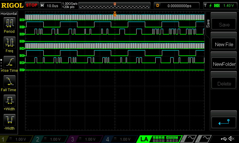
Figure 1 shows the successful I2S transaction according to our outline in the documentation tab on this website. Channels D0-2 are the I2S inputs to the FPGA generated from the MCU. Notice how the channel is set up to be in mono so the data is replicated along the left and right channel. Channels D4-D6 are the I2S outputs from the FPGA after they are modified. Since we are using mono audio our group decided to use the left channel of the FPGA output to showcase the input to the delay buffer. The right channel shows the mixed data and our DAC isolates this channel. This was intended for debugging purposes.
MCU Sample Collection
- Process: The MCU collects samples from the guitar using the analog-to-digital converter (ADC) peripheral.
- Requirement: Because the guitar outputs an analog signal, it must be digitally sampled.
- Rate: A sample rate of 44.1 kHz was chosen to target CD-quality audio. There was an error percentage of about 0.11% since the PLL configuration for the event generator was slightly off.
FPGA DSP Block Implementation
- Implementation: The FPGA incorporates the DSP block to apply a filter on the sampled audio.
- Purpose: This incorporation is required to achieve the chorus effect.
- Library Usage: The DSP library was utilized because the chorus effect requires wave multiplication.
DAC Output Compatibility
- Goal: The DAC must output a signal compatible with a guitar amplifier.
- Status: This goal is not fully met.
- Issues:
- The signal contains a very audible amount of digital noise and 60 Hz pickup.
- The I2S introduces infrequent, periodic distortion to the audio.
- Successes: Aside from the noise, the output is AC-coupled and has the proper amount of gain.
Analog Input Protection and Filtering
- Status: This goal was met.
- Components: The system uses input and output buffers, DC bias, a 4th-order Sallen-Key Butterworth antialiasing filter, and coupling capacitors.
- Protection: Op-amp rails ensure signals greater than 3.3V do not enter the ADC.
- Power: All IC power rails are decoupled with capacitors.
FPGA Testbench Results:
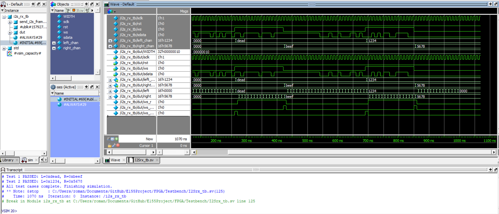
Figure 2 shows a successful transaction from the I2S reciever (rx) to the I2S transmitter (tx) without the DSP module to test signal passthrough. In the signals ‘left_chan’ and ‘right_chan’ the rx module correctly interpreted incoming packet as 0xdeadbeef and 0x123456.

Figure 3 shows a successful tesbench for the Low Frequency Oscillator (LFO), a sub-module of the DSP module. ‘WAVE_o’ Shows the value being read from the sine wave LUT and the frequency of the ‘newValFlag_o’ shows that the value is updating correctly depending on the value of the ‘freqSetting’ to change the speed of the oscillator.

Figure 4 shows a successful testbench for a clock domain crossing from the fast FPGA system to the slower I2S clock. ‘register_o’ is being populated with the values we expect.
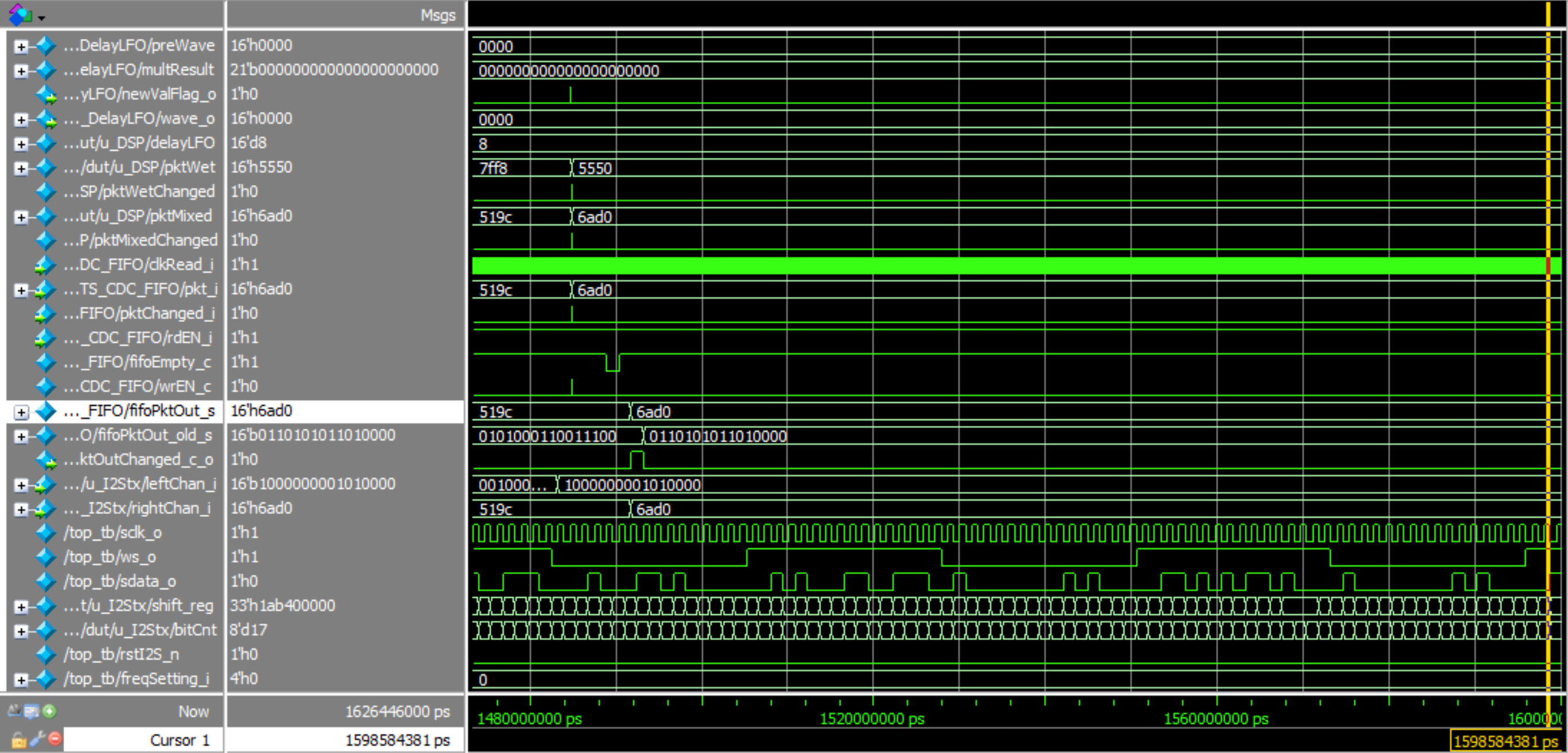
Figure 5 shows a succesful testbench for the Top module where a packet in I2S format was fed in and the output packet was expected to be 0x6ab0 after mixing. This testbench was used to test the async FIFOs for clock domain crossing between the I2S modules and the DSP module, the LFO gen module, the mixer, and the delay buffer. fifoPktOut_s shows the output was as expected.