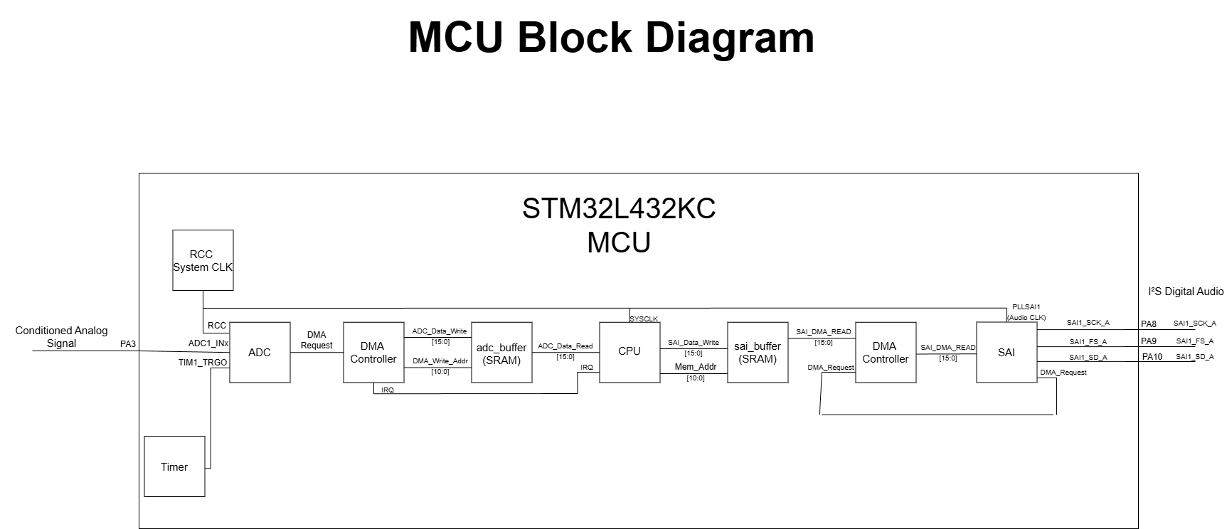
MCU
Summary
ADC
The conditioned guitar signal scaled between 0-3.3V with an offset of 1.65 is passed to channel 8. The ADC is configured in the reset and clock config registers of the MCU to have a speed much faster at sampling than the target audio frequency of 44.1kHz (CD level audio quality). The ADC is triggered by timer 1 to prevent over generation of data that has the chance of overfilling our DMA pipeline or asynch domain crossing FIFO in the FPGA.
DMA
The DMA is configured in a dual buffer mode and it is circular (when a pointer reaches the end of the buffer it circles back to the start). DMA1 is responsible for collecting the sampled data from the ADC and storing it in an ADC buffer without using CPU time. The data is processed in half cycles. When half of DMA1’s ADC buffer is full it transfers the bottom half of the ADC buffer to the SAI buffer while the top half is collecting data. When DMA1 is full the second half of the ADC buffer is transfered to the SAI buffer while the bottom half fills up. Similarly DMA2 transfers data from the SAI buffer to the SAI module to be sent out as an I2S wave. Both are configured in half-word mode (16 bits).
Timer 1
This timer is set up to generate an output event every 44.1kHz. This event is fed to the ADC signaling when the ADC should sample. This is accomplished by clock dividng the system clock down with the Auto relode register.
SAI
This module outputs the ADC data in I2S format to the FPGA. The SAI module uses the PLLSAI clock generator which has the capability of generating common multiples of clock frequencies in audio processing. Our target was 44.1kHz samples per second, so the PLL was set to generate 25644.1kHz. This is because our SAI module has to output a bit clock 3244.1kHz. We want a new sample every 44.1kHz but since the data is serialized (more info under the documentation tab) it takes 32 sclk cycles to transfer one full left and right sample. Thus our SAI module recieves 256*44.1kHz and divides it by 16 to achieve the desired clock frequency for data transfer.
Block Diagram of MCU